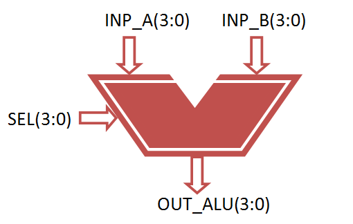
Design a 4-bit ALU that implements the following set of operations with only the following components assume 2s complement number representation no need to implement overflow circuit 1-bit Full-Adders FA 2-input ANDORXOR gates Inverters 21 MUX 0 0 0 0 1 1 1 1 1 1 1 1 0 0 0 0 1 0 1 0 1 0 1 0 Add Subtract Increment. Controlled by the three function select inputs sel 2 to 0 ALU can perform all the 8 possible logic operations.

Verilog Code For Arithmetic Logic Unit Alu Fpga4student Com
Table of 32-bit Arithmetic Logic Unit 31.

. Ac89774 on Mar 29 2017. Design methodology has been changing from schematic design to HDL based design. The shift micro-op operations are often performed in a separate unit but sometimes the shift unit made part of overall ALU.
Include addition subtraction and shifting We proposed arithmetic and logic unit using VHDL structural and dataflow level design. Execute was to design a 1-bit ALU and then combine four of them to create a 4-bit ALU. This paper presents design concept of 4-bit arithmetic and logic unit ALU.
Assign COUT A. Arithmetic-Logic-Unit-ALU-Design-and-Simulation-In-Verilog-and-Proteus Getting Started Verilog Part Getting Started Proteus. This paper presents design concept of 4-bit arithmetic and logic unit ALU.
Since the output of the 4-bit ALU F30 is dependant on the signal M we have two ways of displaying our results. The arithmetic logic and shift units can be combined into ALU with common selection lines. Verified on Xilinx ISE simulator.
Module my_full_adder input A input B input CIN output S output COUT. On the other hand when M1 the output of the 4-bit ALU is a 2s. Mihir Gajjar and Mihir Gajjar 4 - bit ALU using Verilog.
Here verilog HDL was coded using Quartus II 90 version software and 4 bit ALU hardware design was done using Proteus software. This is a 4 bit ALU that Adds and Substract4 Bit Full Adder -httpsyoutubeDVkbizPyde4. We have explored the ALU section of modern CPU using the concept of elementary digital electronics.
Click to share on Twitter Opens in new window. Code 000 2 2s Complement of A op. Today fpga4student presents the Verilog code for the ALU.
Digital Clock manager DCM in Xilinx FPGA. Verification of the designed RTL code using simulation techniques synthesis of RTL code to obtain gate level netlist using Xilinx ISE tool and Arithmetic Logic Unit was successfully designed and. Each module of ALU is divided into smaller modules.
When M0 and the result from the 4-bit ALU is Logic based the result is displayed on an array of LEDs. Mohd Kashif Create Date. Code 100 6 1s Complement of B op.
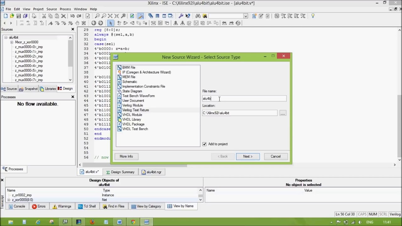
The approach used here is to split the ALU into three modules one Arithmetic one Logic and one Shift module. Full VHDL code for the ALU was presented. In this Video you will learn how to design or implement the 4 bit ALU in verilog using Xilinx Simulator in very simple waySee Code here httpwww2dixco.
1 4 bit Addition op. Department of Electronics and Communication Engineering Athihrii Stephen Sanjay 2016 Page 19 Design and implementation of 32-bit ALU using Verilog 2016 Fig34 Arithmetic Logic Unit 32. Code 001 3 4 bit Add-traction op.
I am supposed to create 4 bit full adder verilog code in vivadoBut when I try to test in the simulationIt give me z and x outputWhich part of code I have to change to get an output in simulation. 131230 07012013 Design Name. Functional Description of 4-bit Arithmetic Logic Unit.
ALU Behavioral Project Name. We proposed arithmetic and logic unit using VHDL structural and dataflow level design. All the modules in arithmetic and.
4-bit ALU Module Name. The testbench Verilog code for the ALU is. Code 011 5 4 input NOR operation using dynamic NOR gate op.
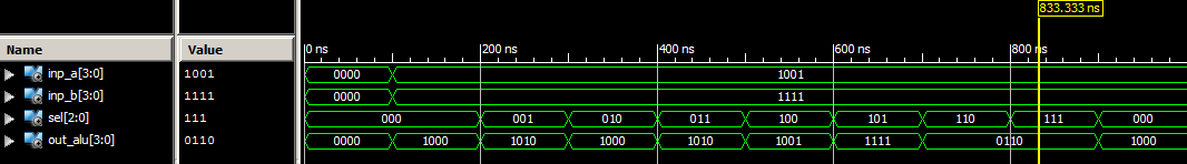
RTL design starting from designing a top level RTL module for 4-bit ALU using hardware description language VHDL. Code 010 4 4 input NAND operation using static NAND gate op. Simulation Result for 4-bit ALU.
There are 6 different functions implemented in this ALU. Design methodology has been changing from schematic design to HDL based design. For shifter unit the selection line S1 is used to select either left or right shift micro-operation.
Assign S ABCIN. The project is a 4-bit ALU in VHDL with a total of 16 operations which includes various arithmetic logical and data calculations performed by coding the ALU in VHDL code. Verilog code for Arithmetic Logic Unit ALU Last time an Arithmetic Logic Unit ALU is designed and implemented in VHDL.
Each module of ALU is divided into smaller modules. 4 - bit ALU using Verilog.
Vhdl Code For 4 Bit Alu

4 Bit Alu Using Vhdl
Vhdl Code For 4 Bit Alu

Vhdl For Fpga Design 4 Bit Alu Wikibooks Open Books For An Open World

Vhdl Code For 4 Bit Alu

Lesson 60 Example 36 4 Bit Arithmetic Logic Unit Alu Youtube
Xilinx Ise 4 Bit Alu Add Subtract Verilog Youtube
4 Bit Alu Design In Verilog Using Xilinx Simulator Youtube
0 comments
Post a Comment